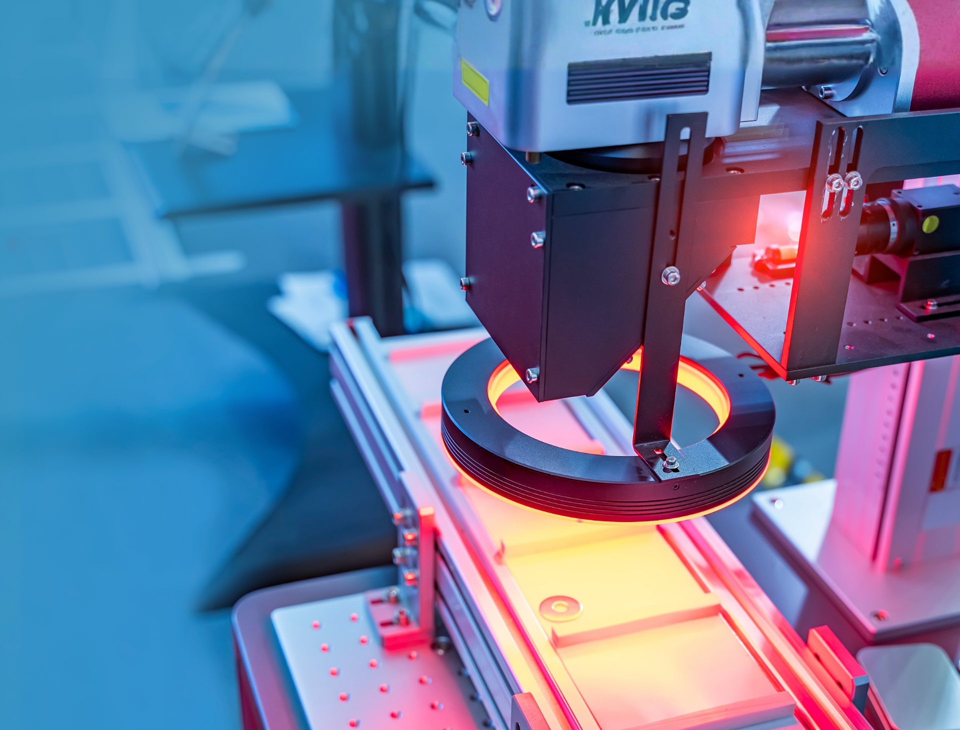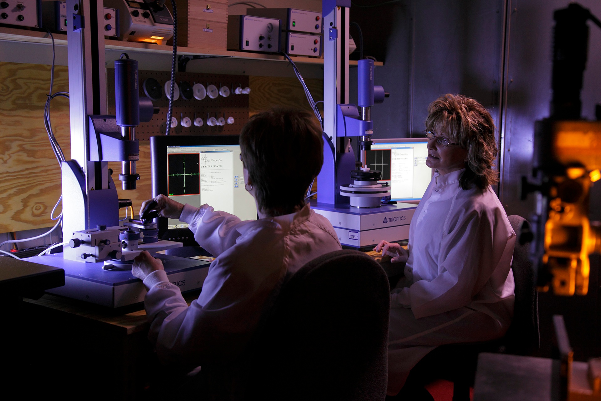


Semiconductor fabs rely on machine vision systems to detect defects, measure critical dimensions and alignment, and improve yield throughout manufacturing. From wafer fabrication and photolithography to advanced packaging and final testing, hundreds of process steps must be monitored with extreme precision. Even though wafer sizes are growing, chip designs and other features are shrinking, making inspection requirements more and more demanding.
Machine vision is a key role in the semiconductor production cycle, especially as the industry is expanding with AI-driven technologies. And with this, the optical components are now just as vital as the camera or software in determining the image quality in a system.
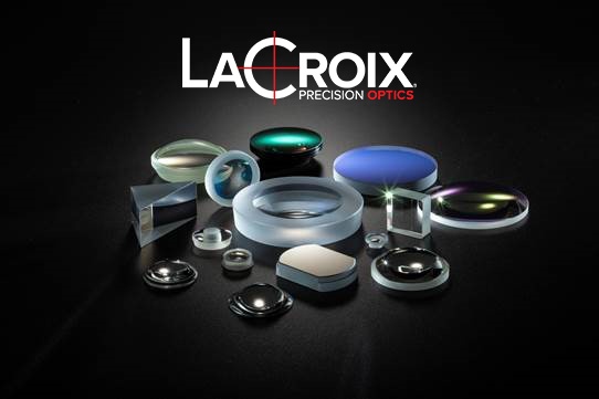
Specialized optics are needed for modern semiconductor inspection that need maximized resolution, contrast, signal-to-noise ratio, and measurement accuracy. Optical building blocks, such as aspheres, telecentric lenses, optical filters, mirrors, and custom coatings are now the backbone to this industry.
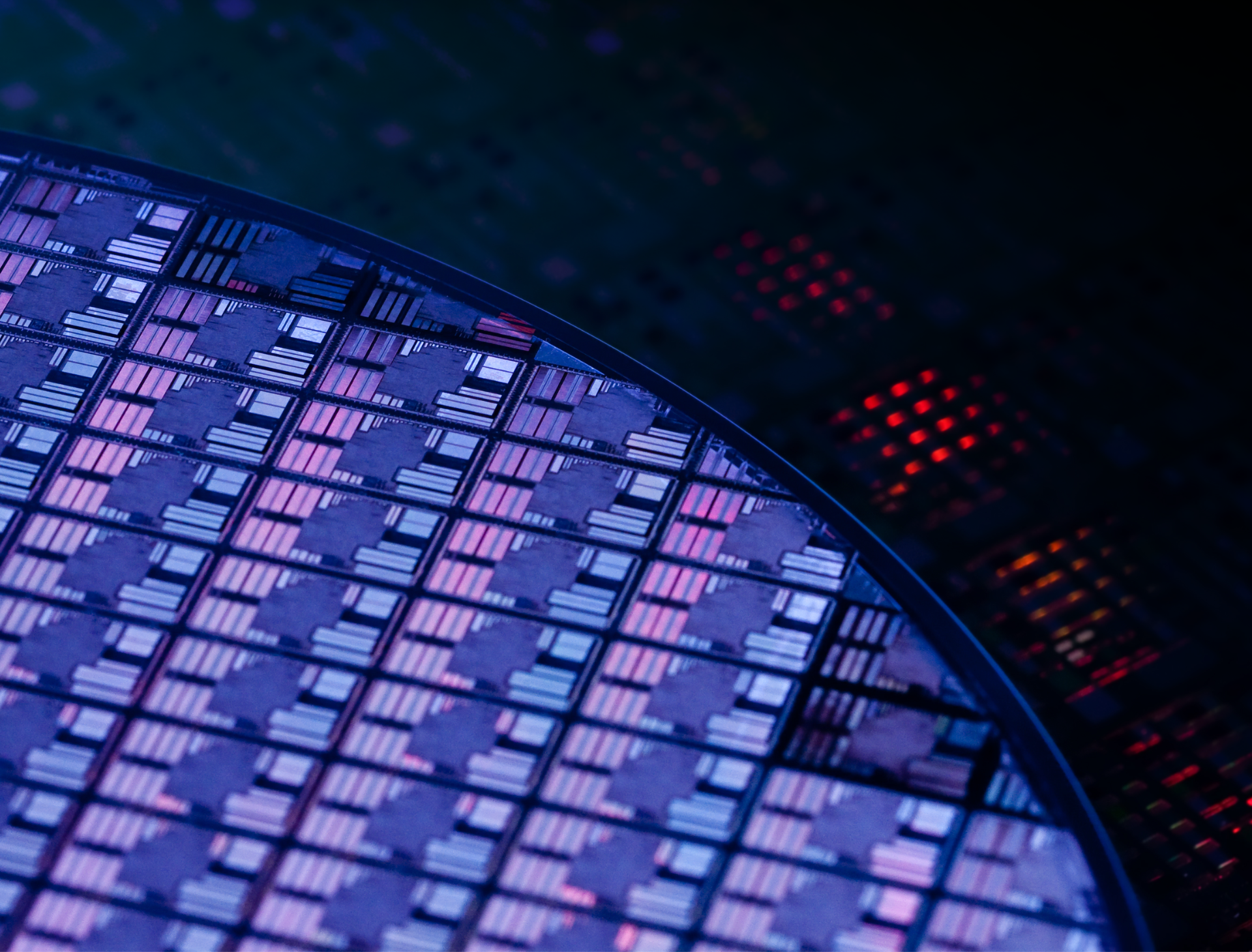
Why Optics are Critical for Semiconductor OEMs
Semiconductor inspection presents challenges that are uncommon in traditional industrial machine vision, including:
-
Maintaining image fidelity across large diameters
-
Detecting defects measured in microns or nanometers
-
Imaging highly reflective surfaces
-
Supporting high-speed automated inspection
-
Operating across visible, ultraviolet, and infrared wavelengths
The semiconductor process needs machine vision systems that detect pattern defects, particles, scratches, contamination, dimensional variations, and process deviations. These requirements place high demands on optical systems.
Engineers can overcome these challenges with specialized lenses, coatings, filters, and beam management components, while enabling evolving inspection tools.
Common Optical Components in Semiconductor Machine Vision Systems
Modern machine vision systems need more than just one specialty optic; they rely on a combination of precision components for their optical stack. Each component plays a specialized role in helping OEMs improve throughput and process control, from maintaining dimensional accuracy and maximizing image sharpness to improving illumination uniformity and enabling imaging across ultraviolet, visible, and infrared wavelengths.

Working together, these optics help semiconductor OEMs detect smaller defects, improve process control, increase yield, and support modern high-performance inspection platforms. Advanced semiconductor inspection systems increasingly rely on specialty optics, including telecentric lenses, beam splitters, filters, prisms, specialty coatings, and custom optical assemblies, to improve imaging performance and inspection accuracy beyond what standard catalog optics can provide.
| Component | Primary Impact | Common Applications |
| Aspheric Lenses | Reduce spherical aberration and improve edge-to-edge image quality | Wafer inspection, defect imaging, metrology |
| Telecentric Lenses | Eliminate perspective error and maintain dimensional accuracy through enhanced edge contrast and magnification | Critical dimension measurement & alignment |
| Beam Expanders & Splitters | Improve illumination uniformity | Laser inspection, scanning systems |
| Optical Filters | Enhance contrast and isolate wavelengths | Surface inspection, contamination detection, spectral filtering |
| Prisms & Wedges | Redirect and manipulate light paths | Alignment systems, compact optical assemblies |
| Multi-Element Objectives | Maximize resolution and minimize distortion | High-resolution inspection and metrology |
| Mirrors | Redirect light while maintaining optical performance | Laser inspection tools, folded optical paths |
| Custom Coatings (AR, SWIR, and DUV) | Improve transmission, reduce unwanted reflections, optimize wavelength performance, and enhance image contrast across visible, infrared, and ultraviolet systems | Defect detection, wafer inspection, photolithography monitoring, through-silicon inspection, low-light imaging, optical sensor performance enhancement |
How Each Optical Component Solves a Semiconductor Inspection Challenge
Aspheric Lenses Improve Resolution Without Increasing Complexity
Traditional spherical optics often introduce spherical aberrations, but Aspherical lenses correct them, improving image quality at the edges of the field of view. Complementing the shrinking sizes of semiconductor devices, aspheres often allow designers to reduce the number of lens elements while still maintaining exceptional performance.
Telecentric Lenses Enable Accurate Metrology
Semiconductor manufacturers rely on precise dimensional measurements throughout production. Telecentric lenses maintain consistent magnification regardless of object position, eliminating perspective distortion and improving repeatable processes. This makes them a cornerstone of semiconductor machine vision systems.
Beam Splitters and Expanders Support Complex Optical Architectures
Advanced inspection systems integrate multiple imaging paths, illumination, and compact system layouts. Beam splitters and expanders provide designers with the flexibility needed to route and manipulate light without sacrificing precision.
Beam expanders are often used to create more consistent illumination across surfaces in scanning and metrology processes, while beam splitters support higher-throughput inspection architectures by enabling multiple camera integration or synchronized illumination and imaging along the same optical axis.
Optical Filters Improve Contrast and Defect Visibility
Many semiconductor defects are only visible when certain wavelengths are emphasized. Optical filters help isolate specific wavelengths while blocking unwanted light, improving contrast, defect detection, signal-to-noise ratio, and, overall, real-time monitoring.
Prisms, Wedges, and Mirrors Enable Complex Optical Systems
Packaging constraints often are the determining requirement for an optical design. Today’s systems must be compact while still maintaining performance. Specialty prisms, wedges, and mirrors help enable multiple imaging paths or illumination geometries while being tailored for tight optical architectures, an essential factor for machine vision systems.
Specialty Coatings Expand What Machines Can See
Coatings are often the difference between a good image and a great one. Anti-reflective coatings reduce stray reflections and improve signal-to-noise ratio, while SWIR and DUV coatings enable imaging outside the visible spectrum to reveal defects and features that traditional optics cannot detect.
Why Semiconductor OEMs Are Moving Towards Custom Optics
Historically, system integrators relied on catalog optics to reduce costs and accelerate development in their machine vision programs, but the semiconductor industry has greater performance demands than ever. Standard optics are just not meeting their specific, unique requirements anymore.
Manufacturers are now turning to custom optical solutions designed around the end application’s and operating environment’s performance requirements. Specialty optics and custom assemblies help improve signal-to-noise ratio, accuracy, and inspection performance for advanced machine vision.
One main driver is the expansion of AI-powered inspection systems. Machine learning algorithms that power modern technology are sensitive to image inconsistencies. Even small alignment errors or distortions can affect inspection accuracy. Custom optical assemblies allow for tightly controlled decentration and tilt, improving MTF and enabling high-quality, consistent imaging data.
But that’s not the only reason. Other factors contributing to the custom optic demand include:
-
OEMs needing to tailor components to system-level constraints, such as multiple imaging paths, integrated illumination systems, compact footprints, and operation across specialized wavelength ranges
-
Manufacturers looking to ensure repeatable precision and scalability to match industry expansions, often with optical partners that provide design-for-manufacturability (DFM) support
-
Demand for long-term product stability and supply chain resilience with optics developed around application-specific needs
Custom optics are now a strategic subsystem that influences the overall performance, not just an individual component. As semiconductor inspection requirements continue to evolve, custom optical solutions provide greater flexibility to optimize the entire machine vision platform to meet manufacturability and AI-readiness standards.
Specialty Optics Mean Specialized Machine Vision Systems
Semiconductor devices are more complex, more compact, and more performance-driven. Machine vision systems must keep pace with the changing tolerances and higher resolution requirements. And that starts with picking the right optical stack.
From aspheres and telecentric lenses to beam management optics, filters, mirrors, and advanced coatings, each optical component contributes to the precision and repeatability that semiconductor manufacturers demand. Specialty optics are providing the flexibility to optimize and future-proof every part of an OEMs system. They just need to find the right optical partner.
Build Your Next Semiconductor Vision System with LaCroix
LaCroix partners with semiconductor equipment manufacturers to develop and manufacture precision optical components and assemblies optimized for demanding machine vision applications. No matter if you are developing a new inspection platform or enhancing an existing system, contact our application experts to tailor your optical components to your project today.